

MacBook Charger Components and Working Principle
The MacBook Charger is mainly composed of the following components:
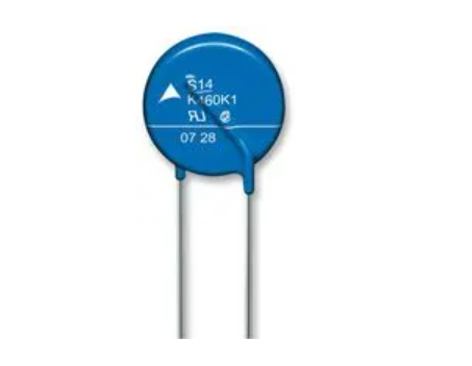
- Varistor,The feature of the varistor is that when the external voltage is too high, the resistance of the varistor becomes very small rapidly, and the fuse connected in series with the varistor is blown to protect other circuits from being burned out.

2. Fuse,The specification is 3A/250V, when the current in the circuit is too large, the fuse will blow to protect other components.
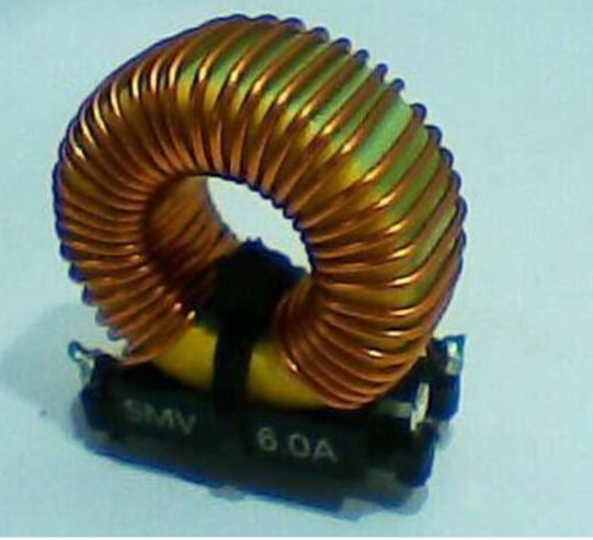
3. Inductor coil,The main feature is to reduce electromagnetic interference.
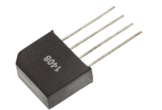
4. Rectifier bridge,The specification is D3SB, the function is to change 220V AC into DC.
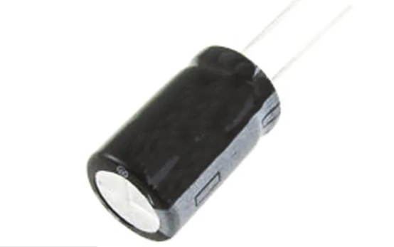
5. Filter capacitor,The Specification is 180uF/400V,The feature is to filter out the AC ripple in the DC power to make the circuit work more reliably.
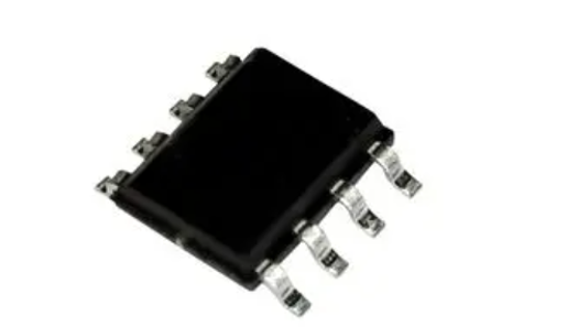
6. Operational amplifier IC (integrated circuit), an important part of protection circuit and voltage regulation.
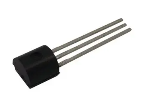
7. Temperature probe,It is used to detect the internal temperature of the power adapter. When the temperature is higher than a certain set value (different brands of power adapters have slightly different set temperature thresholds), the protection circuit will cut off the voltage output of the adapter to protect the adapter. not damaged.
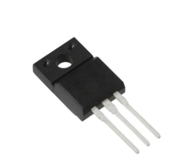
8. High power switching tube,It is one of the core components in the switching power supply. The switching power supply can work “one on and one off”, and the switching tube is indispensable.
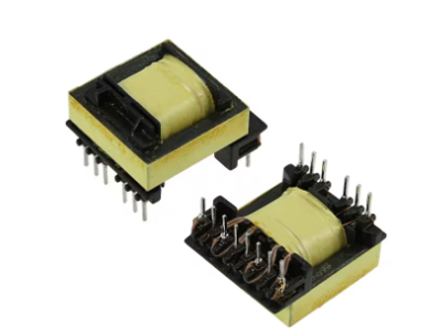
9. Switching transformer,One of the core components in switching power supplies.
10. Secondary rectifier,The function is to convert low-voltage alternating current into low-voltage direct current. In IBM’s power adapter, the rectifier tube is often operated in parallel by two high-power to obtain a larger current output.
11. Secondary filter capacitor, The specification is 820uF/25V, there are two in total, which can filter out the ripple in the low-voltage direct current.

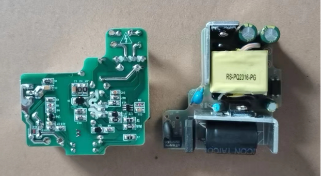
In addition to the above components, there are adjustable potentiometers and other resistance-capacitance components on the circuit board. Our PCBA is as attached.
The other side of PCBA for MacBook Charger as below.
Working principle
The adapter converts 220V AC voltage to 19V DC voltage with an output current of 3A. The 220V AC voltage is rectified by D2 and filtered by C1 to obtain a 300V DC voltage. This voltage is applied to the D terminal of the MOSFET switch Q1 (K2543) through the 1, 2 winding of the switch transformer T1. Another path goes through R4 to obtain a startup voltage of about 17V for ICI (KA3842) pin 7, and a 5V reference voltage is generated from the internal reference voltage generator of ICl and output from pin 8. At this time, its internal oscillator starts oscillating and outputs a pulse width modulation (PWM) from pin 6, which drives the switch Q1 to work in the on/off state. The output current of the D terminal of Q1 generates an induced voltage on the primary winding of the switch transformer T1, which is coupled to the secondary winding of T1 through the magnetic core. The induced voltage generated on the 5, 6 winding of the secondary winding is rectified and filtered by the Schottky diode Q2 and capacitor C4 to obtain a 19V DC voltage output.
In order to ensure stable output voltage, the output terminal is sampled by R13 and R14, and the sampling voltage is compared and error amplified by the three-terminal adjustable shunt reference IC3 (TL431) and then driven by the optocoupler IC2 (PC817) to amplify the error voltage and send it to the internal pin 1 of IC1 (KA3842). The width of the output pulse from pin 6 is changed by the internal PWM circuit to change the switching time of Q1, thereby achieving the purpose of adjusting the output voltage. After such a feedback control process, the output voltage is finally stabilized at 19V.
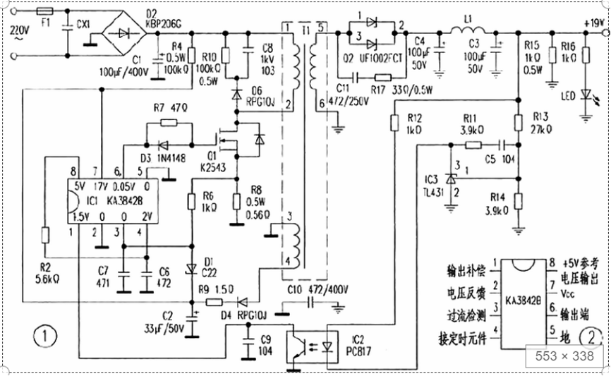
Several overvoltage and overcurrent protections are also provided in this circuit: The induced voltage on the 3, 4 winding of the switch transformer primary winding is rectified and filtered by D4 and C2 to obtain a voltage of about 17V, which is sent to pin 7 of IC1 to maintain the normal operation of ICI (the voltage supplied to pin 7 by the 300V voltage through R4 is only used as a startup voltage because the current is small). When the output voltage rises due to some reason, this voltage will also rise. When the voltage rises above 22V, the voltage regulator diode D1 will break down, causing the voltage at the overcurrent protection end of pin 3 of IC1 to rise above 1V. At this time, the internal PWM output from pin 6 of IC1 will be cut off, causing the circuit to stop working, achieving the purpose of overvoltage protection.
When the current of the switch Q1 is too large due to some reason, the voltage at the ends of the overcurrent sampling resistor R8 connected to the S terminal of Q1 will rise. When the voltage rises to make the voltage at pin 3 of IC1 higher than 1V, the output from pin 6 of IC1 will also be cut off, achieving the purpose of overcurrent protection.
The R10, C8, D6 connected to the D terminal of the switch Q1 form a peak absorption circuit, which absorbs the peak induced pulse generated on the 1, 2 winding of T1 during the cutoff period of Q1 to prevent Q1 from being breakdown.